Convert delay time to trace length
Work back from a propagation delay to the trace length that produces it. You get the answer for both an outer layer (microstrip) and an inner layer (stripline).
History
Formula
Outer layer (microstrip): εeff = (εr+1)/2 + (εr−1)/2 × (1+10h/w)^−0.5
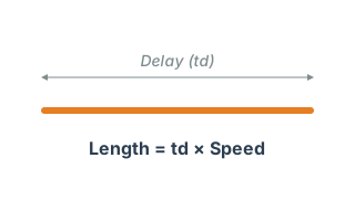
L = TD × c / √εeff
Design notes
This answers "how many millimetres of trace do I need for X ps of delay?" — the question that comes up constantly when length-matching a fast interface.
For DDR4-3200:
• One bit period ≈ 313 ps
• Skew budget ≈ ±20 ps → you have to match to about ±1.4 mm
An outer layer has a lower effective permittivity than an inner one, so the same length delays the signal less. Worth remembering when you choose a layer.
When you need this
Once timing analysis tells you that you are 200ps short, this converts that into how many millimetres of trace to add. It gives you the serpentine length directly.
What it is for
Timing is reasoned about in picoseconds; layout is done in millimetres. This bridges the two. When setup or hold margin is short, it tells you how much serpentine routing to add, or how much to remove to get back inside the budget.
Inner and outer layers need different lengths for the same delay, so you can also decide which layer to put the meander on.
Worked example: fixing a hold violation with routing
- Timing analysis reports a 200ps hold shortfall.
- FR-4 (εr = 4.3), trace width 0.2mm, dielectric height 0.1mm.
- Entering 200ps gives 28.93mm on an inner layer, 32.91mm on an outer layer.
- The inner layer needs 4mm less, so it wins if area is tight.
- Add about 5% margin — roughly 30mm — and re-run timing analysis to confirm.
Alternatives to adding trace
- Shift the clock phase. If the device has a PLL or DLL, you can often move several hundred picoseconds without touching the board. No area cost, so try this first.
- Add a series resistor. Working against the load capacitance it slows the edge and delays the effective arrival. It also degrades the edge, so this is not an option for fast signals.
- Change layer. Outer layers are faster, so simply moving a net inward buys roughly 80ps per 100mm.
- Reduce drive strength. Where the device allows it, a slower edge arrives later and helps EMI at the same time.
Serpentine routing costs area and disturbs impedance at every fold. Exhaust the alternatives first.
Common mistakes
- Routing exactly the calculated length. Manufacturing and εr variation move this by a few percent. Add margin, then confirm with analysis.
- Bunching the meander mid-net. For reflection purposes it is better to place serpentine routing close to the receiver.
- Stretching one half of a differential pair. Correct for fixing intra-pair skew, but differential impedance is disturbed over that section. Keep the correction as short as possible and preserve pair spacing.
Frequently asked questions
Where should serpentine routing go?
Why do inner and outer layers need different lengths?
How many millimetres is one via worth?
Standards and references
- IPC-2141A — Delay design for high-speed traces.
- Howard Johnson, "High-Speed Signal Propagation" — Coupling and effective delay in serpentine routing.
Last updated: 2026-08-29