PCB design calculators
Online calculators that run in your browser, aimed at hardware and PCB engineers. They cover characteristic impedance, propagation delay, trace resistance and parasitics. Some fields accept SI prefixes (k, M, G, u, n, p).
Latest articles
-
The inductor voltage: seen from which terminal? V = L·dI/dt and switching supplies
2026-09-19
An inductor is "the part that can't change its current suddenly" — it will put out whatever voltage it takes to keep the current flowing. The V in V = L·dI/dt is exactly that "voltage produced to hold the current," and it flips direction depending on whether the current is rising or falling. That flip is both the spike you get when you switch off, and the working principle of a boost converter.
-
Passive vs. active filters: which to build, and the pitfalls by application
2026-09-19
"Active is just higher performance" isn't right. An active filter can't be used on a power rail or at RF, and a passive filter alone isn't enough ahead of an ADC. Before what a filter passes or blocks, the signal's frequency, power, and impedance decide which topology you're even allowed to use.
-
Op-amp circuits from the ground up: watching inverting, non-inverting, and VCVS (Sallen-Key) in motion
2026-09-19
Op-amp circuits look like a large zoo of variations, but there's only one way to read any of them: "with negative feedback in place, the two input terminals sit at the same voltage," and "no current flows into the input terminals." With just these two rules, you can trace how the voltage moves in an inverting circuit, a non-inverting circuit, or even a 2nd-order filter.
-
Why is a clock crystal 32.768kHz? The reason it isn't built to output 1Hz directly
2026-09-15
32768 is an odd-looking number because it's 2 multiplied by itself 15 times. Pass that frequency through a circuit that does nothing but "halve it," fifteen times over, and out comes a pulse exactly once a second. So why not just build a crystal that vibrates once a second to begin with? The reason that can't be done is exactly the reason this frequency was chosen.
-
Microstrip trace width is decided by the stack-up
2026-09-14
"I want 50 ohms, so tell me the trace width" cannot be answered as asked. The width is set by the thickness of the dielectric under that trace. The stack-up has to be fixed before the width can be, and the fab still fine-tunes that width in the end.
TOOL Circuit simulators in your browser — build a circuit and watch the waveforms with CircuitJS1, or run an IBIS model through a PCB trace.
-
Propagation speed on a PCB from permittivity
Calculate signal propagation speed on a PCB in ps/mm from the relative permittivity. For timing analysis in high-speed design.
-
Trace resistance, heating, inductance and parasitic capacitance
Calculate the resistance, inductance, dissipation and parasitic capacitance of a PCB trace. For high-current and high-speed design.
-
Via and through-hole parasitics
Calculate the parasitic inductance and capacitance of a PCB via. For return path design on fast signals and for decoupling.
-
Skin effect
Calculate skin depth — how far current penetrates a conductor at a given frequency.
-
Characteristic impedance — microstrip (outer layer)
Calculate the characteristic impedance of a microstrip line, single-ended and differential, and pick a trace width for your stack-up.
-
Lumped or distributed
Find the boundary between lumped and distributed behaviour: the limiting trace length for a frequency, or the limiting frequency for a length.
-
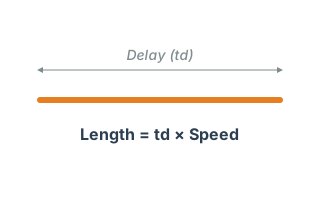
Convert delay time to trace length
Work out the trace length that corresponds to a given propagation delay. For length matching and skew adjustment.
-
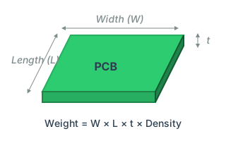
PCB weight
Calculate the weight of a printed circuit board. Get the laminate and copper mass from the outline size, layer count and copper thickness.
-
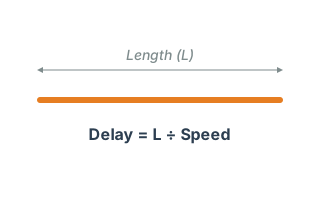
Convert trace length to delay time
Calculate the propagation delay of a PCB trace from its length. For length matching and timing analysis.
-
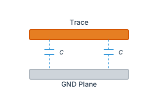
Trace capacitance
Calculate the parasitic capacitance of an inner-layer PCB trace (stripline) in pF. For signal integrity and filter design.