Convert trace length to delay time
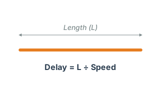
Work out the propagation delay of a trace from its length. The reverse of "convert delay time to trace length".
History
Formula
Outer layer (microstrip): TD = L × √εeff / c [ps]
εeff = (εr+1)/2 + (εr−1)/2 × (1+10h/w)^−0.5
Design notes
Turn a trace length into a delay. This is the number behind length matching on any fast interface.
For DDR SDRAM:
• DDR4-3200: one bit period ≈ 313 ps
• Skew budget ≈ ±20 ps → length has to match to about ±1.4 mm
Working the delay budget back into a length tolerance before you set up length-matching rules in the CAD tool saves a lot of iteration later.
When you need this
For checking what a 12mm length difference actually costs in picoseconds during a layout review, or for turning the length report out of your CAD tool into timing. It reports outer and inner layers together, so nets that change layer can be compared directly.
Why there are two answers
The same physical length takes different times depending on the layer. A stripline is enclosed by dielectric, so its effective permittivity is the laminate εr. A microstrip has air above it, lowering the effective permittivity and speeding the signal up.
The outer-layer figure is derived from the trace width w and dielectric height h. The smaller w/h is — narrow trace, thick dielectric — the more field escapes into the air and the faster the signal travels. Wide and thin approaches the inner-layer value.
Worked example: matching across layers
- FR-4 (εr = 4.3), trace width 0.2mm, dielectric height 0.1mm.
- Net A runs 100mm on an inner layer: 691.2 ps.
- Net B runs 100mm on an outer layer: 607.7 ps.
- Identical lengths, but 83.5 ps apart — 0.8% of a 100MHz clock period.
- To match B to A you would have to stretch the outer-layer net to 691.2 ÷ 6.077 ≈ 114mm.
Most CAD length-matching features match physical length only. On nets that change layer, this entire difference survives.
Common mistakes
- Taking serpentine routing at face value. Tightly spaced meander segments couple to each other, so the real delay is a few percent short of the geometric length. Keep the spacing between folds at least 3–4 times the trace width.
- Not counting vias. A via through a 1.6mm board is roughly 10ps. Three layer changes is 30ps, equivalent to about 4mm of trace.
- Ignoring package-internal routing. Bond-out lengths inside a BGA differ by several millimetres between pins. For fast memory interfaces, subtract the package lengths the silicon vendor publishes before matching on the board.
Frequently asked questions
Which figure should I use?
Do width and height only affect the outer-layer result?
How much margin should serpentine routing have?
Standards and references
- IPC-2141A — Effective permittivity for microstrip and stripline.
- JEDEC JESD79-4 (DDR4) — Skew allowances within address and data groups.
Last updated: 2026-08-29