Trace capacitance
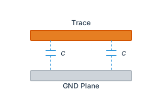
Parasitic capacitance of a PCB trace. This is the capacitance an inner-layer trace (a stripline) has to the ground planes above and below it. The two distances can be set separately.
History
Formula
(W: trace width, L: length, h₁: distance to the ground above, h₂: distance to the ground below)
With h₁ = h₂ = h this is the same as C = εr × L × (0.441 + W/2h) / (30×π×0.3).
Design notes
An inner-layer trace sits between two ground planes and has capacitance to both. That capacitance slows the edge rate, and slower edges are how fast signals degrade.
When the two distances differ (an offset stripline), the closer plane sets most of the capacitance. On an asymmetric stack-up, check whether only one side is a thin prepreg.
What it does to the design:
• More capacitance means a longer rise time
• Together with the driver's output impedance it forms an RC filter
• On a fast bus it is a capacitive load that eats into your bandwidth
Ways to reduce it: narrow the trace, move the planes further away, or move to a laminate with a lower permittivity.
When you need this
For the high-impedance nodes where the trace itself loads the circuit — feedback dividers, high-resistance analogue inputs, crystal circuits, capacitive touch sensor runs. Where a few picofarads change the behaviour, trace capacitance is not negligible.
What is calculated
The capacitance of an inner-layer trace (stripline) to the reference planes above and below. The two distances are entered separately, so asymmetric stack-ups are handled.
It is a parallel-plate term plus a fringing term for the field at the trace edges. When the trace is narrow relative to the plane spacing, the fringing contribution dominates.
Where it bites
- Switching converter feedback dividers. With divider resistors in the hundreds of kilohms, a few picofarads add phase shift and the loop oscillates. Keep FB routing short and do not pour ground under it.
- Crystal load capacitance. A few extra picofarads shift the oscillation frequency. If you need ppm accuracy, include trace capacitance in the load calculation.
- High-resistance analogue inputs. 5pF on a 1MΩ input is a 5µs time constant — too slow for fast sampling.
- Reset and boot-strapping pins. A 100kΩ pull-up on a long trace gives a slow edge that can miss the latch window at start-up.
Worked example: a feedback trace
- 0.2mm wide, 50mm long inner-layer trace, 0.1mm to each ground plane, εr = 4.3.
- The calculator gives about 11 pF.
- With divider resistors of 470kΩ and 100kΩ, the equivalent resistance at the FB pin is about 82kΩ.
- The time constant is 82kΩ × 11pF ≈ 0.9µs, placing a pole at about 176kHz.
- For a 500kHz converter with a 50kHz target loop bandwidth, that pole is not negligible. Shortening the trace to 10mm cuts the capacitance by five and pushes the pole out to 880kHz.
Common mistakes
- Pouring ground under a sensitive node. Copper added for noise immunity becomes capacitance. Under feedback and high-impedance nodes it is often better to deliberately clear the plane.
- Not counting vias and pads. A via is 0.3–0.5pF and a component pad 0.5–1pF. These accumulate even on short nets.
- Ignoring adjacent traces. This calculates capacitance to the planes only. A trace running alongside adds coupling capacitance and a crosstalk path.
Frequently asked questions
Can I use this for surface traces?
How do I reduce trace capacitance?
How do I calculate crystal load capacitance?
Standards and references
- IPC-2141A — Stripline capacitance and impedance.
- IPC-2221B — General design standard; layer construction and routing.
Last updated: 2026-08-29