FPGA/MCU I/O Buffer Standards & Drive Strength
A reference on FPGA/MCU I/O buffer standards (LVCMOS, LVTTL, etc.) and drive strength, with a calculator that estimates rise time from drive current and load capacitance.
History
Formula
(V: supply voltage [V], I: drive current [mA], C: load capacitance [pF])
Frequency where this transition exceeds 10% of the period: f ≈ 100 / tr [MHz]
Design notes
This treats the output stage as an ideal constant-current source — a rough, order-of-magnitude model. Real buffers have slew-rate control and saturation behavior, so datasheet numbers can differ by tens of percent. The guide below covers the basics of LVCMOS/LVTTL, how vendors configure them differently, and when to use 8mA vs. 12mA drive strength.
When you need this
For when you run into an unfamiliar setting name for I/O buffers — Xilinx's IOSTANDARD=LVCMOS33, STM32's GPIO speed, or a "port drive capability" register on a TI or Renesas MCU — and want to know what it actually means electrically. This page covers what LVCMOS/LVTTL specify and how to choose a drive strength (mA), and estimates the rough rise time from drive current and load capacitance.
What LVCMOS and LVTTL actually are
Both are single-ended, CMOS-output digital I/O standards referenced to GND. What separates them is mostly how the switching thresholds are defined: LVCMOS uses thresholds proportional to the supply (roughly VIH ≈ 0.7×VCC, VIL ≈ 0.3×VCC), while LVTTL uses fixed thresholds inherited from classic TTL regardless of supply (roughly VIH ≈ 2.0V, VIL ≈ 0.8V). At 3.3V these two land close enough together that datasheets often just lump them as "LVTTL/LVCMOS compatible."
Both are defined per supply-voltage class in JEDEC's JESD8 series — LVCMOS33 (3.3V), LVCMOS25 (2.5V), LVCMOS18 (1.8V), LVCMOS15 (1.5V), LVCMOS12 (1.2V) and so on. Lower supply voltages mean a proportionally smaller absolute noise margin, so don't drop the voltage class casually on a noisy board.
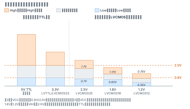
This is the key difference. LVTTL (and, in practice, 3.3V LVCMOS33) uses fixed thresholds inherited from TTL (VIL max 0.8V, VIH min 2.0V), so those absolute numbers don't move when the supply changes. LVCMOS at 2.5V and below uses thresholds proportional to the supply (roughly 30%/70% as a rule of thumb), so the thresholds slide down together with the supply voltage. In the diagram, notice how the threshold band on the right three bars shifts downward as the voltage drops.
At 1.8V or 1.2V, the fixed VIH minimum of 2.0V would actually exceed the supply voltage itself — it simply can't work. That's exactly why low-voltage devices never offer "LVTTL" as an option and always specify an LVCMOS voltage class instead. It's not a coincidence that LVTTL and LVCMOS33 are treated as interchangeable at 3.3V — both reference the same JEDEC spec, JESD8-B.
Always use the exact thresholds and output levels from your device's datasheet. The numbers here are typical ballpark figures for the standard, not guaranteed values for any specific part.
Other standards in the same family
Beyond LVCMOS/LVTTL, there's a whole range of standards chosen for different jobs. Grouped roughly by family:
| Family | Examples | Characteristics |
|---|---|---|
| Single-ended, fixed threshold | TTL (5V) / LVTTL (3.3V) | Fixed thresholds inherited from TTL (VIL max 0.8V, VIH min 2.0V). Doesn't work below about 1.8V supply. |
| Single-ended, proportional threshold | LVCMOS33/25/18/15/12/10 | Thresholds scale roughly 30%/70% with the supply. Every low-voltage device uses this family — the default for FPGA/MCU IOSTANDARD. |
| Single-ended, low-swing bus | GTL / GTL+ | Roughly 0.8V swing, VREF-referenced, open-drain, wired-OR capable so many receivers can share one bus. Used on the Pentium Pro-era front-side bus and SCSI; largely retired today. |
| Single-ended, reference-voltage (memory) | SSTL2 / SSTL18 / SSTL15, HSTL | VREF-referenced, even lower swing and faster than LVCMOS. These map to DDR / DDR2 / DDR3 memory interfaces respectively; HSTL shows up in high-speed parallel I/O on networking chips. |
| Differential | LVDS (TIA/EIA-644), LVPECL/PECL, CML | Both use the voltage difference between two wires, so they resist ground shifts and common-mode noise. LVDS is a low-power general-purpose differential link; PECL/LVPECL and CML show up in clock distribution and optical interfaces. |
| Differential, display/bus variants | RSDS, mini-LVDS, BLVDS | LVDS variants tuned for a specific job. RSDS/mini-LVDS are used inside LCD panels; BLVDS is built for multipoint bus connections. |
| Open-drain bus protocols | I2C, 1-Wire | Leaves the High level to an external pull-up, letting multiple devices share one wire. The thresholds themselves usually follow the same VIL/VIH as LVCMOS/LVTTL. |
This calculator and guide mostly cover the top two rows — single-ended, voltage-referenced LVCMOS/LVTTL, the default for general-purpose GPIO on FPGAs and MCUs. Memory interfaces and high-speed serial links call for one of the other families in the table.
How different vendors name and configure this
| Vendor | Where it's configured | Summary |
|---|---|---|
| Xilinx (7 Series / UltraScale) | IOSTANDARD / DRIVE / SLEW in the XDC | IOSTANDARD selects the voltage class (LVCMOS33/25/18/15/12, etc.). DRIVE picks 4/8/12/16/24mA drive strength and SLEW picks FAST/SLOW slew rate, per pin. |
| TI (Sitara/MSP, etc.) | Pin-mux (IOMUX) registers | Some devices offer a few drive-strength steps (e.g. normal/high), others are fixed. Check the I/O buffer characteristics table in the datasheet. |
| Renesas (RX/RA) | Port drive capability register (PMR/DSCR, etc.) | Many parts let you switch "high drive" vs. "standard" per pin, but high-drive is often limited to specific dedicated pins. |
| STM32 (ST) | GPIO OSPEEDR (output speed) | No Xilinx-style mA drive-strength selection. Instead you pick Low/Medium/High/Very High slew rate. Current rating itself is essentially fixed per pin (typically around 8mA as a ballpark, with some high-voltage/FT pins rated higher). |
What the vendor differences mean in practice
Even for the same "LVCMOS 3.3V" buffer, the granularity of what you can configure differs by vendor. Xilinx lets you pick current and slew rate independently, each with several steps; STM32 only lets you pick a slew-rate "speed," with current essentially fixed. When reading a datasheet, first figure out whether it exposes "drive strength in mA" or "speed in discrete steps."
Where the 8mA / 12mA numbers came from
The reason "8mA" and "12mA" still show up as drive-strength options on modern FPGAs and logic ICs traces back to 5V-era TTL logic (the 74 series). TTL output stages were asymmetric: sink capability in the Low state (IOL) was substantial, while source capability in the High state (IOH) only needed to be tiny, because of how TTL input stages were structured — they only drew meaningful current while held Low.
Standard 74-series parts (74/74LS) were specified with IOL ≈ 8mA, which turned out to be just enough to sink the current from several TTL inputs plus some trace capacitance on a shared bus while still meeting the VOL spec (below roughly 0.4–0.5V). For heavier loads — backplanes, buses with many receivers — stronger variants (74S/74F/74ALS) offered IOL of 12mA, 20mA, 24mA, and this "8/12/16/20/24mA" step pattern became the industry's shared vocabulary.
CMOS logic (74HC/74AC onward) and modern FPGA/MCU output stages are push-pull, sourcing and sinking roughly equal current in either direction. Even so, the available drive-strength options still follow that historical 8/12/16/24mA step pattern — the phrase "how many mA can it drive" was already the industry's vocabulary from the TTL era, and it simply carried over into the CMOS age.
More is not automatically better here. Raising drive strength speeds up the edge, which worsens simultaneous-switching noise (SSO), crosstalk, and overshoot/ringing on any trace that isn't properly terminated. Not choosing more drive strength than you need is part of EMI control.
A rule of thumb for choosing
- Light load, short trace (a few pF to ~10pF, short routing). 4–8mA with SLEW=SLOW is the default. Don't make the edge faster than it needs to be — keeps noise and EMI down. General-purpose GPIO, buttons, LED control all fall here.
- A bus with several receivers, or a relatively long trace. Bump up to roughly 12–16mA so the extra load capacitance still reaches VOH/VOL fast enough.
- Fast clocks, or signals that must meet a specific setup/hold requirement. You'll need SLEW=FAST and higher drive strength, but on a trace that isn't designed as a controlled transmission line this produces significant reflections and ringing. Match the characteristic impedance and add series termination if needed.
- Battery-powered designs where current matters. Higher drive strength also raises the peak (and so average) switching current. Leave lightly-loaded signals at a weak drive strength.
About the calculator: estimating rise time from drive current
Treating the output stage as an ideal constant-current source, the time to charge the load capacitance is estimated as tr ≈ 0.8 × C × V / I (0.8 is a simplified factor standing in for the 10%–90% transition). Real buffers have output impedance, saturation behavior and slew-rate control circuitry, so treat this purely as an order-of-magnitude estimate.
Example: at 3.3V with 8mA drive and 20pF of combined trace + input-pin capacitance, this calculator gives a rise time of about 6.6ns. That transition starts to exceed 10% of the period above roughly 15.2MHz — past that, you'd need either more drive strength or less load capacitance.
Doubling the drive current from 8mA to 16mA on the same load roughly halves the rise time (to about 3.3ns) — in this formula, drive strength and transition time are inversely proportional.
Frequently asked questions
Should I pick LVCMOS or LVTTL?
What's the difference between SLEW (slew rate) and DRIVE (drive strength)?
Does STM32 have an "8mA/12mA" style drive-strength setting like Xilinx?
Will this calculator's rise time match a datasheet measurement?
Standards and references
- JEDEC JESD8 series — LVTTL/LVCMOS thresholds and output levels per supply-voltage class.
- TIA/EIA-644 (LVDS) — Low-voltage differential signaling standard.
Last updated: 2026-08-30